As well as coming in scalable shapes and sizes, LED displays are also manufactured using different techniques. With a plethora of LED display technologies and manufacturing methods now available, we want to ensure you are empowered to make the right choices when picking an LED display solution.
Here we explore the three main pixel technologies on the market today, their standout features, the benefits and the different use cases to ensure optimum performance for your next project. We will also explore a technique called Glue on board (GOB) and its benifits.
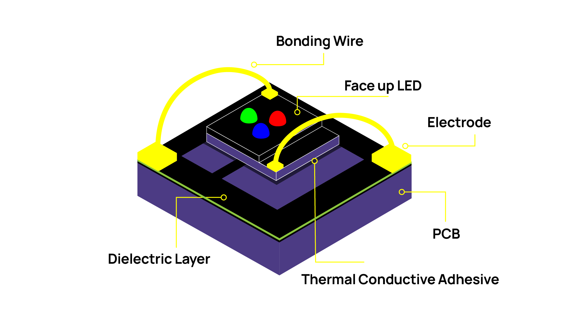
SMD technology is where the LED packages are mounted onto the surface of a printed circuit board (PCB).
Each SMD is made up of one red, one green and one blue LED which are assembled into a lamp, divided into similar wavelengths in batches, then packaged on the module. The combination of the RGB LEDs allow for the creation of white light and form one pixel. Hundreds or thousands of SMD’s are then mounted onto a module/tile.

As the market has matured, SMD has become the most cost-effective choice of LED pixel technology, offering great value for money. This manufacturing process ensures a high level of precision and colour accuracy with a consistent and reliable output. As the technology has evolved, pixel pitches have got smaller and as a result LED displays have increased in resolution, opening up a new era for display technology.
SMD pixel technology is, as of today, the most popular option for both indoor and outdoor applications. In recent years pixel pitches have got smaller and so the use of SMD technology can be found in live events, corporate lobbies, retail signage, roadside billboards and many more!
The seamless, bezel free nature of LED displays' versus traditional LCD video wall panels makes it the ideal replacement for legacy large format displays like projection and video walls that are reaching end of life, due to improved energy efficiency and vast improvements in image quality.
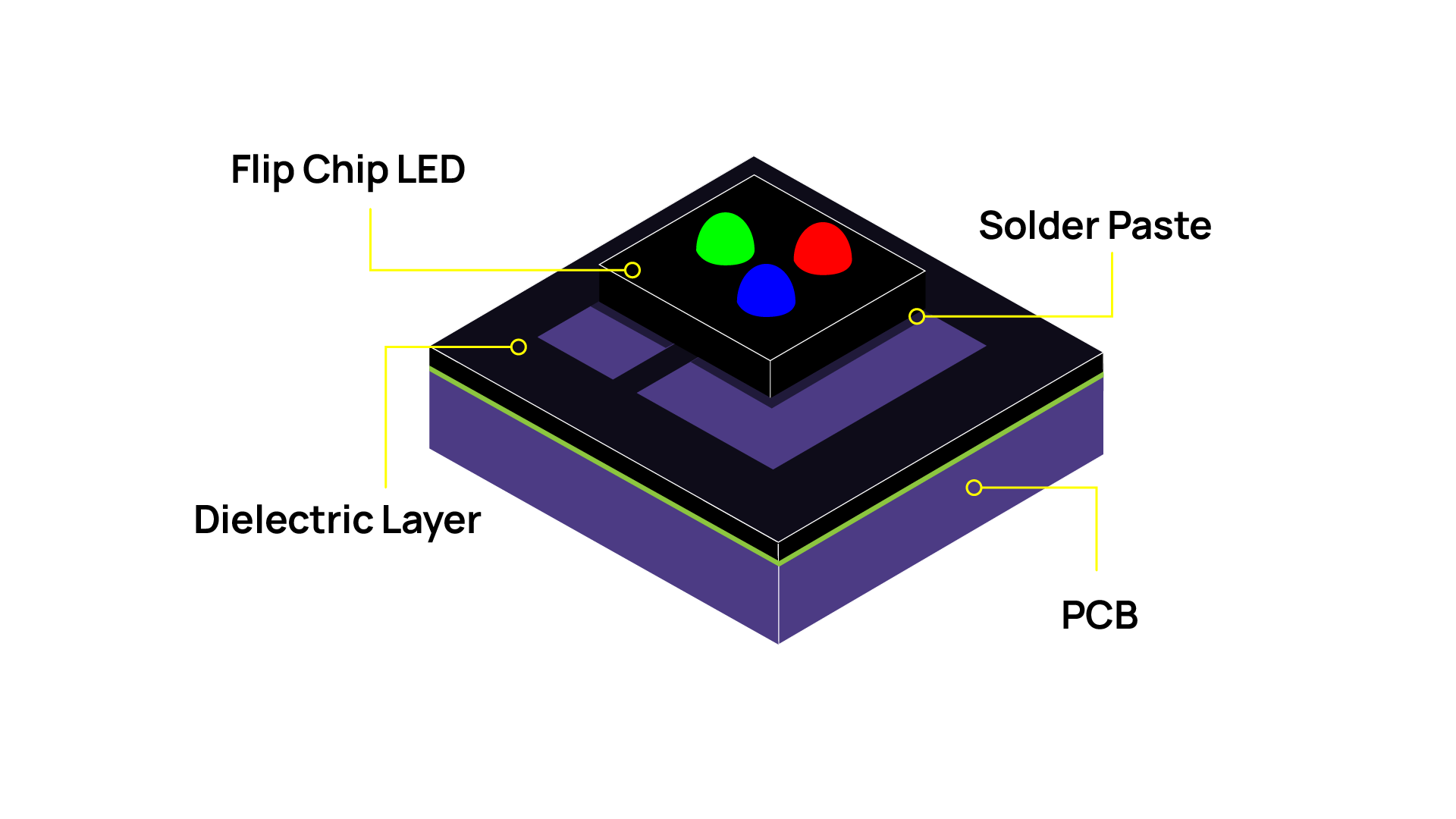
The Flip Chip SMD pixel manufacturing process literally involves taking the RGB diodes and flipping them, removing the need for the copper bonding wires. Flip Chip is called Flip Chip SMD, as the lamp is still soldered/ mounted to the PCB.

By eliminating the diode's wire bonds it results in drastically reduced electrical resistance, vastly improving energy efficiency and reducing running costs. In terms of performance, Flip Chip ensures superior picture quality with greater uniformity.
Flip Chip is also capable of much higher Nit output with brightness's of up to 2000 or 4000nits making it the ideal choice for high bright areas. This is achieved because the Flip Chip manufacturing process delivers a more efficient way of driving the LEDs and a display that is cool to the touch.
When thinking about ROI, Flip Chip ticks lots of boxes due to its reliability, reduced running costs and increased performance etc, but there is another critical benefit that is usually overlooked.
As mentioned above, reduced heat output is a key benefit when working in confined spaces where additional air conditioning may be required to cool the space if you were to use SMD pixel technology or other forms of visual display.
Flip Chip displays are ideal for environments that require extra brightness but also want the small pixel pitch options and visual performance of SMD displays with the added benefit of running much more efficiently. This includes shop windows, reception atriums or indoor areas with high ambient light.
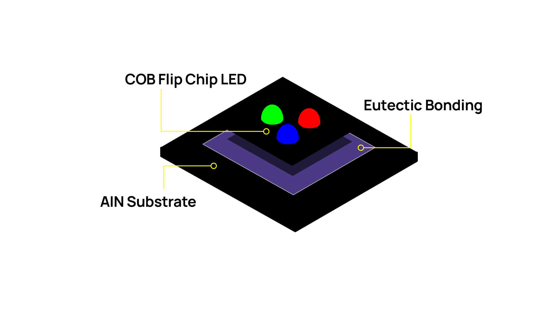
COB LED manufacturing is the process of embedding the pixels directly into the PCB, effectively printing them. Compared to SMD or Flip Chip, this allows the individual diodes and pixels to be packaged much closer together, resulting in even finer pixel pitches and greater uniformity.

Due to the close proximity of each LED and their position on the PCB, COB displays are capable of delivering very high resolution images with pixel pitches as low as 0.65mm, advanced colour reproduction (DCI-P3), 1,000,000:1 contrast ratios and wide viewing angles for off-axis viewing as well as offering vast energy efficiency benefits.
The encapsulation process used in COB displays helps to protect the LED chips from damage, prolonging lifespan and enhancing reliability as dry or broken solder points are vastly reduced. Many compare the module finish to that for a GOB module as the pixels are protected by a top coat of resin.
Its wide colour gamut and fine pixel pitch options make it ideal for immersive spaces where close-up viewing is paramount, as well as for high-end installations that require high-resolution imagery, including retail environments, high-end hospitality, immersive spaces and home cinema.
Glue On Board is a type of finish applied to the module that is available with any SMD or Flip Chip LED Studio product. This uses a patented epoxy resin to encapsulate the PCB and pixels offering robust protection from accidental or intentional harm.

When GOB is combined with SMD or Flip Chip pixel technologies, this greatly increases the durability and reliability of the display by enhancing the protection around each pixel. It makes the display impact-resistant, dustproof, waterproof, and IP-rated up to IP65. Additionally, it aids in heat dissipation by increasing the display's surface area, resulting in a more uniform display. GOB should always be a consideration in areas with heavy footfall when screens are at ground or touchable levels.
At LED Studio, we have also developed a proprietary GOB using a special compound with the resin, which allows us to create a blue light filter. This filter prevents eye strain during extended viewing periods, making it ideal for control rooms or heavily used displays.
The increased robustness makes GOB LED displays ideal for digital signage located at ground level and in heavy footfall areas, including retail, transportation terminals and hospitality venues.
The enhanced reliability, excellent contrast ratio and IP rating also extends its uses to DOOH for kiosks and billboards (when paired with Flip Chip High Bright) that require minimal maintenance and deliver exceptional performance.
The EDGE
EDGE Pro
GENESIS
AEGIS Pro
AEGIS
As you can see, each LED manufacturing process has its own advantages and disadvantages, depending on the application and the size of the display.
As technology continues to advance, we will remain at the forefront of developing new methods and innovations to solve complex challenges and deliver superior performance in all spaces.
Note: Diagrams are simplified for illustration purposes.